Researchers at Chitkara University in the Indian State of Punjab have proposed an electrostatically-doped back-contact design for perovskite-based solar cells that overcomes the fabrication and performance challenges associated with conventional sandwiched architecture using charge transport layers.
The researchers performed numerical simulations and modeling to arrive at an electrostatically-doped metal-perovskite-metal back-contact solar cell structure that offered a significant improvement of 59.4% in power conversion efficiency (with an absolute reported value of 4.13%) over the previously proposed structures in the domain, where the absolute reported value was 2.59%.
Dr Rahul Pandey, Dr Jaya Madan and Dr Rajnish Sharma from the university’s VLSI Center of Excellence carried out the research. Their work has been recently published in a scientific journal from the Institute of Electrical and Electronics Engineering (IEEE), IEEE Transactions on Electron Devices..
Dr Rajnish, who leads the VLSI Center of Excellence at Chitkara University, told pv magazine, “In an earlier reported design of back-contact metal-perovskite-metal solar cell architecture, the carrier collection only relied mainly on the Schottky field across the perovskite layer and hence the performance, particularly in terms of open-circuit voltage, was limited by the work function difference between the self-assembled monolayer (SAM)-modified gold contacts.”
“The numerical study by our researchers established that an electrostatically-doped dipole-field-assisted metal-perovskite-metal back-contact perovskite solar cell structure could overcome the limitations of dipole-field-assisted metal-perovskite-metal back-contact perovskite-based solar cell structures.”
The researchers proposed placing two additional electrodes beneath the glass substrate to provide the polarity difference and to create an electrostatically doped p-n junction and corresponding built-in potential inside the perovskite layer near the glass substrate. The induced built-in potential offered additional support to light-generated charge carriers for the enhanced collection probability and helped overcome the limitations of the device reported earlier.
While back-contact dipole-field-assisted metal-perovskite-metal solar cell reported earlier delivered the conversion efficiency of 2.59%, the design reported by Chitkara University researchers, where electrostatic doping has been introduced, provided a conversion efficiency of 4.13%.
Design
The Chitkara University researchers’ study findings may pave the way for the development of ‘transport layer-free’ electrostatically-doped, scalable, and low-cost perovskite-based solar cells in the future.
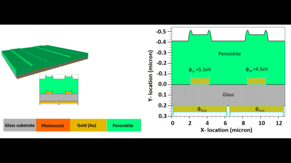
Their proposed design consists of a perovskite layer deposited onto a glass substrate having self-assemble-monolayer-modified gold-patterned electrodes on one side and polarity electrodes on the backside. The polarity electrodes allow for electrostatic control on the polarity carriers generated due to light photons falling on the solar cell structure’s active area. The dipole field due to front electrode and electrostatic potential due to polarity electrodes combine to enhance the charge extraction, enhancing the values of collection probability and open-circuit voltage.
Quantitatively, 14.2 mA.cm-2, 659 mV, and 44.2% absolute values were reported for short-circuit current density (JSC), open-circuit voltage (VOC) and fill factor (FF)—a notable improvement of 24.6%, 17.5% and 9.1%, respectively, over existing structures in which these values were reported as JSC (11.4 mA.cm-2), VOC (561 mV) and FF (40.5%).
For the ideal expected functioning of any solar cell structure, all 100% generated carriers in terms of electrons and holes should find an easy path to successfully traverse to the structure’s end electrodes and contribute toward charge buildup. However, most of the structures in vogue struggle to ensure that and maximum of the generated carriers get sacrificed to various kinds of losses happening in the device.
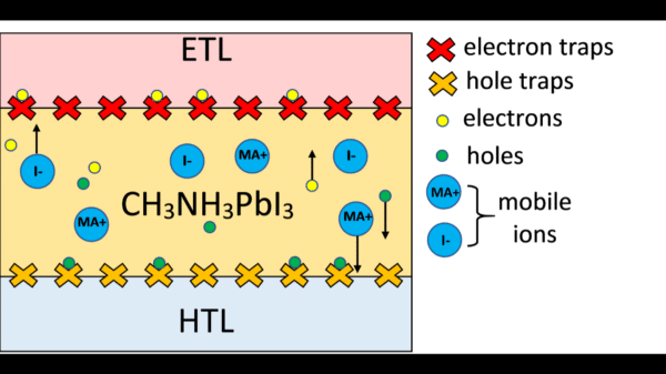
In conventional perovskite solar cells, a thin active layer of perovskite is sandwiched between two charge transport layers, an electron transport layer (ETL) and a hole transport layer (HTL). The creation of suitable electric field at the electron transport layer/perovskite and perovskite/hole transport layer interface helps in overall better collection of carriers. But their deployment may also cause performance degradation if side effects like enhanced recombination of carriers at the traps are not managed well. A pictorial representation indicating these losses has been drawn as below.

Besides these functional issues, it has never been that easy to fabricate perovskite-based solar cell structures, and issues faced on that front due to their moisture-sensitive nature, possible shortening between electrodes due to pinholes and minimization of series resistance lead to additional losses.
Researchers at Chitkara University worked to possibly overcome all these issues by numerically simulating and proposing a device structure without the presence of charge transport layers and opting for a back-contact design.
To get rid of charge transport layers, the team proposed the placing of the polarity electrodes with workfunction Фm,p = 5.25 eV and Фm,n = 4.35 eV beneath the glass substrate to create an additional built-in field for the overall enhancement of internal electric field between the back contacts and obtained very encouraging results. Field inducted this way was seen to increase the carriers’ collection probability and improve the conventional structure’s power conversion efficiency.

Dr Rajnish concluded, “Perovskite has been showing immense potential for the future generations of solar cells. This is one area where there has been almost an exponential growth in achieving the high values of PCE. However, like in all research endeavors, many issues still need to be resolved. We have shown in this work that with the simple addition of two electrodes beneath the glass substrate, one can harvest the benefits of having an electrostatically-doped p-n junction leading to the corresponding built-in potential inside the perovskite layer near the glass substrate.”
“We look forward to support coming in from government funding agencies to make an indelible mark on the international research roadmap in this field,” he added.
This content is protected by copyright and may not be reused. If you want to cooperate with us and would like to reuse some of our content, please contact: editors@pv-magazine.com.


By submitting this form you agree to pv magazine using your data for the purposes of publishing your comment.
Your personal data will only be disclosed or otherwise transmitted to third parties for the purposes of spam filtering or if this is necessary for technical maintenance of the website. Any other transfer to third parties will not take place unless this is justified on the basis of applicable data protection regulations or if pv magazine is legally obliged to do so.
You may revoke this consent at any time with effect for the future, in which case your personal data will be deleted immediately. Otherwise, your data will be deleted if pv magazine has processed your request or the purpose of data storage is fulfilled.
Further information on data privacy can be found in our Data Protection Policy.