U.S.-based wafer manufacturer 1366 Technologies has confirmed plans for a 2 GW solar wafer and cell production facility in India. The unit is being planned under the Indian government’s production-linked incentive (PLI) scheme, which aims to drive deployment of every stage of the solar supply chain, from polysilicon to module manufacturing.
A spokesperson for the company told pv magazine it is exploring manufacturing opportunities for its ‘direct wafer’ production process in India and the business said it is also seeking module partners.
“The Indian government has made domestic solar manufacturing a priority and our technology is particularly well suited for the Indian market,” said the 1366 spokesperson. “Direct wafer manufacturing can immediately deliver the lowest cost of electricity in a single-junction device for India’s utility market, and it underpins an economically feasible, high-efficiency, tandem product for global leadership.”
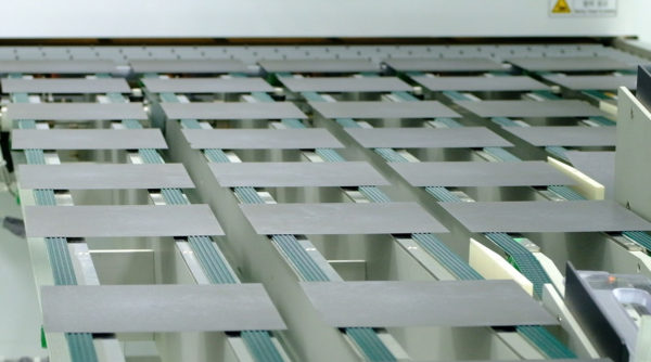
Kerfless
The direct wafer process is a kerfless wafer technique, meaning it does not require silicon ingots to be sawn into wafers, a time-consuming process that wastes material as silicon dust. Instead, 1366’s technology forms wafers directly, using molten silicon. The company claims its direct wafer process offers the world’s lowest wafer production cost, translating into cell and module competitiveness.
The direct wafer approach has long held big hopes for the industry and the company operates a demonstration facility in Bedford, Massachusetts, where most of its technological developments were achieved. One such was a 20.3% cell efficiency level recorded in August 2017 in a Q Cells Q.antum cell which incorporated passivated emitter rear contact (PERC) technology and 1366 wafers. That record, 1366 Tech said at the time, was achieved on a pilot line using standard processes seen in mass production.
This copy was amended on 24/06/21 to reflect 1366 Technologies is planning a wafer and cell facility, rather than just wafers, and that it is seeking solar module, rather than cell partners.
This content is protected by copyright and may not be reused. If you want to cooperate with us and would like to reuse some of our content, please contact: editors@pv-magazine.com.








1 comment
By submitting this form you agree to pv magazine using your data for the purposes of publishing your comment.
Your personal data will only be disclosed or otherwise transmitted to third parties for the purposes of spam filtering or if this is necessary for technical maintenance of the website. Any other transfer to third parties will not take place unless this is justified on the basis of applicable data protection regulations or if pv magazine is legally obliged to do so.
You may revoke this consent at any time with effect for the future, in which case your personal data will be deleted immediately. Otherwise, your data will be deleted if pv magazine has processed your request or the purpose of data storage is fulfilled.
Further information on data privacy can be found in our Data Protection Policy.