From pv magazine 11/2021
Amorphous silicon (a-Si) deposition is the core process for HJT cells and the key to their electrical properties. The process completes the p-n junction through chemical vapor deposition of intrinsic hydrogenated amorphous silicon (a-Si:H), p-type a-Si:H (around 5 nm), and n-type a-Si:H (around 5 nm).
Plasma enhanced chemical vapor deposition (PECVD) is currently the mainstream process for a-Si:H layers, as it has higher stability and equipment maturity. To improve the short circuit current of HJT cells, manufacturers are testing deposition on microcrystalline silicon (uc-Si:H). Since uc-Si:H thin film grows rather slowly and has issues related to vertical evenness, very high-frequency chemical vapor deposition (VHF-CVD) might be adopted. Some manufacturers are also evaluating hot wire chemical vapor deposition (HWCVD) for mass production, as it delivers high deposition efficiency and better passivation results.
Wafer texturing
The texturing process, which is conducted before cell deposition, includes the removal of saw damage and light-trapping structures, and the cleaning of the wafer surface, reducing recombination losses. There are three process routes: RCA cleaning (hydrogen peroxide + ammoniacal nitrogen), hydrogen peroxide-ozone cleaning, and pure ozone cleaning.
RCA cleaning performs better at removing particles and chemical impurities from the wafer surface. However, the method will be eliminated gradually due to the higher consumption of chemicals and higher costs of nitrogen deposition. Hydrogen peroxide-ozone treatment is currently the most widely adopted method, which can effectively reduce nitrogen emissions and costs. Import into China of ozone and domestic production of additives enables HJT texturing costs to be identical with PERC. Pure ozone treatment is not commonly used due to its lower ability to clean organic matter.
TCO film deposition
As the conductivity of the a-Si:H is poor, adding a 100 nm layer of transparent conductive oxide (TCO) film between the electrode and a-Si:H layer can increase charge carrier collection. TCO films can deliver high electrical conductivity, reduce reflection, and protect the a-Si:H layer. The most widely used TCO coating techniques are magnetron sputtering (PVD) and reactive plasma deposition (RPD).
Despite better photoelectric properties of indium tungsten oxide (IWO), fewer manufacturers adopt RPD due to patent and cost issues. S.C New Energy, a Chinese equipment supplier that uses this technique, claims that IWO film processed by RPD has 0.3% higher ITO efficiency. PVD, however, has no patent issues and has better stability and lower costs, meaning it is popular among equipment suppliers.
As the TCO process step continues to be optimized, consumption of ITO has reduced to around 20 mg/W. With indium recycling and the introduction of aluminum zinc oxide (AZO) on the rear side, ITO consumption is likely to drop further.
Metallization matters
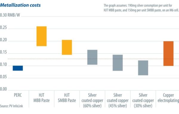
Bifacial HJT cells require two to three times the consumption of silver paste compared with PERC. Coupled with heavy dependence on imports into China of low-temperature paste, high costs induced by the metallization step have become the biggest barrier facing HJT.
The most widely discussed approaches to reduce metallization costs are silver-coated copper paste and copper electroplating. Silver-coated copper receives higher acceptance, as it can be done without modifying production lines. It is reported that 30% copper maintains cell efficiency, but is less competitive in terms of cost. If the percentage of copper could be brought to 45% or higher, metallization costs of HJT could reach the level of PERC or even lower. However, a higher percentage of copper will lead to a decrease of cell efficiency by 0.1% to 0.3%, and the big problem is the reliability of copper exposure.
Manufacturers are investigating electroplating techniques, but for now, it remains in the research stage. While copper electroplating itself only costs CNY 0.03-0.05 ($0.0047-0.0078/W), if including costs of the PVD seed, photomask preparation, and texturing, the cost of metallization is estimated at CNY 0.15/W, which is not cost-competitive, but there is much room for improvement.
Production efficiency
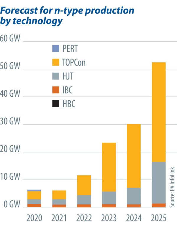
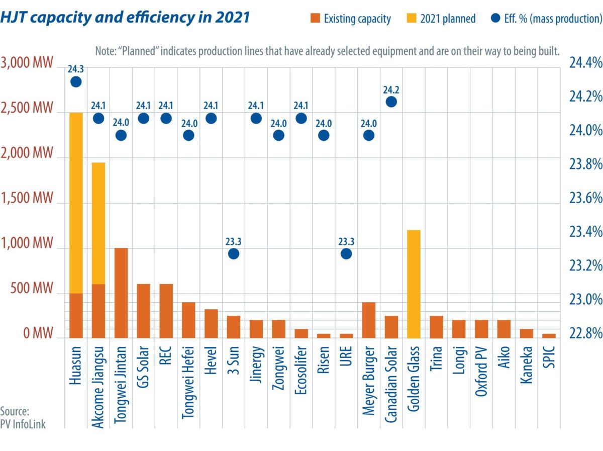
HJT has drawn plenty of market attention already. Recently, Tongwei’s 1 GW-HJT project was completed, Huasun’s 1.2 GW project commenced construction, JA Solar announced plans to install pilot lines, and Akcome expanded gigawatt-scale production capacity. Meanwhile, Ming Yang Smart Energy Group, HaiTai New Energy, and China Resources Power will engage in HJT as well. Statistics show more than 80 GW of HJT production capacity has been planned thus far, and we expect to see 10 GW come online in 2022.
HJT cell efficiencies have passed the 24% mark. There are still various process routes to push this higher, such as gettering process and the substitution of a-Si:H for uc-Si. Despite higher dependence on equipment for improving efficiencies, equipment suppliers and manufacturers both claim that they will achieve better than 25% efficiency in mass production in 2022, as equipment and costs continue to be optimized. HJT technology saw no yield rate issues, with manufacturers claiming 97% and beyond of yield rates, close to that of PERC cells.
Fewer process steps, better yield rates, and high cell efficiency give HJT technology a bright outlook. But subject to higher manufacturing costs and the inability to widen its lead in efficiency over p-type PERC and n-type TOPCon cells, HJT production and capacity will not grow significantly in the short term.
HJT manufacturers are actively adapting to the trend for larger wafers, accommodating newly added and modified production lines with the M10 and G12 formats. HJT capacity and production output will continue to grow in one to two years, but the pace hinges on cost reductions, with metallization being the pivotal segment. After technologies of silver-coated copper pastes and copper electroplating reach maturity, HJT technology will see more and more gigawatt-scale capacity expansions. It’s expected that mass production will not take place until after 2024, as it requires one to two years to optimize costs.
About the author
Derek Zhao has more than 10 years of experience in the PV industry. Prior to joining InfoLink Consulting, he worked for Tier-1 solar equipment suppliers, BOM manufacturers and vertically integrated companies, providing technical support, as well as market, product, and technology management. He now serves as a senior analyst at PV InfoLink, which is a division of InfoLink Consulting. His work involves the analysis of technology routes across the PV supply chain, offering clients up-to-date insights about manufacturing technologies and advice on relevant strategies
The views and opinions expressed in this article are the author’s own, and do not necessarily reflect those held by pv magazine.
This content is protected by copyright and may not be reused. If you want to cooperate with us and would like to reuse some of our content, please contact: editors@pv-magazine.com.



By submitting this form you agree to pv magazine using your data for the purposes of publishing your comment.
Your personal data will only be disclosed or otherwise transmitted to third parties for the purposes of spam filtering or if this is necessary for technical maintenance of the website. Any other transfer to third parties will not take place unless this is justified on the basis of applicable data protection regulations or if pv magazine is legally obliged to do so.
You may revoke this consent at any time with effect for the future, in which case your personal data will be deleted immediately. Otherwise, your data will be deleted if pv magazine has processed your request or the purpose of data storage is fulfilled.
Further information on data privacy can be found in our Data Protection Policy.