From pv magazine Global
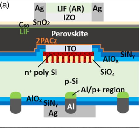
Scientists in Germany have developed for the first time a tandem perovskite silicon solar cell based on an n+-type polysilicon on oxide (POLO) front junction and a passivated emitter and rear contact (PERC) side.
“This is an important achievement, since PERC silicon cells on p-type silicon are the ‘workhorse’ of photovoltaics, with a market share of about 50% of all solar cells produced worldwide,” the scientists said. “Our bottom cells comprise all components of industrial PERC cells, except for the substitution of phosphoryl chloride (POCl3) diffusion by low-pressure chemical vapor deposition (LPCVD) of in situ n+-type p-doped poly-Si,” they further explained, noting that the process flow for this bottom cell is compatible with commercial mainstream PERC technologies.
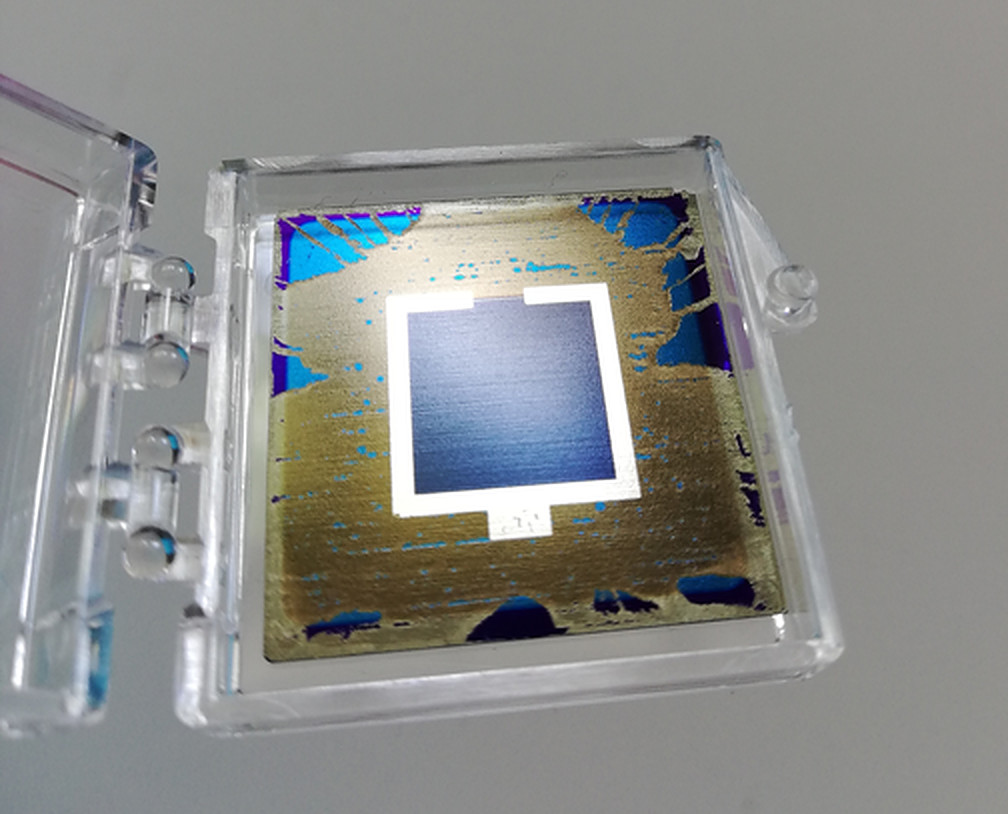
The cell was fabricated with a p-type gallium-doped M2 Czochralski (Cz) wafer with 156.75 μm edge length and a diameter of 210 mm, with the stacks of Al2O3 and SiNx being deposited on both sides of the wafer. “The rear-side 15 nm Al2O3/100 nm SiNx stack serves for passivation just as in an industrial PERC cell,” the research team explained. “The front-side 10 nm Al2O3/40 nm SiNx stack passivates the perimeter region around the active cell area. It also serves the rather fundamental purpose to stabilize the POLO junction passivation during the subsequent firing process and is therefore removed in the active area only after firing.”

Image: HZB, RRL Solar, Creative Commons Licence CC BY 4.0, https://bit.ly/358rI9p
The perovskite top cell was developed with a p−i−n device architecture and a triple-halide perovskite with a bandgap of 1.68 eV known as CsFAPb(IBrCl)3. “As its thickness strongly influences the current density generated in the top cell, adapting its fabrication process is crucial to achieve current matching between the subcells,” the academics emphasized. “To reduce the current mismatch, we deposit a thinner perovskite layer by increasing the spin-coating speed to 5000 revolutions per minute (rpm) resulting in a film thickness of about 470 nm.”
The two-terminal perovskite−POLO−PERC tandem solar cell achieved a power conversion efficiency of 21.3% and the scientists said this proof-of-concept tandem device has potential for further efficiency improvements. “For this purpose, one could adapt the surface of the silicon wafers and thus quickly increase the efficiency to about 25%,” said the research’s corresponding author, Silvia Mariotti.
The German group believes the efficiency of these devices may reach much higher values through adjustments in the perovskite thickness and bandgap that were not considered so far. “Based on our experimental findings and supporting optical simulations, we identify major process enhancements and estimate a PCE potential of 29.5%,” it further explained.
A full description of the cell can be found in the study Monolithic Perovskite/Silicon Tandem Solar Cells Fabricated Using Industrial p-Type Polycrystalline Silicon on Oxide/Passivated Emitter and Rear Cell Silicon Bottom Cell Technology, published in RRL Solar. The research group comprises scientists from the Institute for Solar Energy Research (ISFH) and the Helmholtz-Zentrum Berlin für Materialien und Energie (HZB).
This content is protected by copyright and may not be reused. If you want to cooperate with us and would like to reuse some of our content, please contact: editors@pv-magazine.com.


By submitting this form you agree to pv magazine using your data for the purposes of publishing your comment.
Your personal data will only be disclosed or otherwise transmitted to third parties for the purposes of spam filtering or if this is necessary for technical maintenance of the website. Any other transfer to third parties will not take place unless this is justified on the basis of applicable data protection regulations or if pv magazine is legally obliged to do so.
You may revoke this consent at any time with effect for the future, in which case your personal data will be deleted immediately. Otherwise, your data will be deleted if pv magazine has processed your request or the purpose of data storage is fulfilled.
Further information on data privacy can be found in our Data Protection Policy.