From pv magazine global
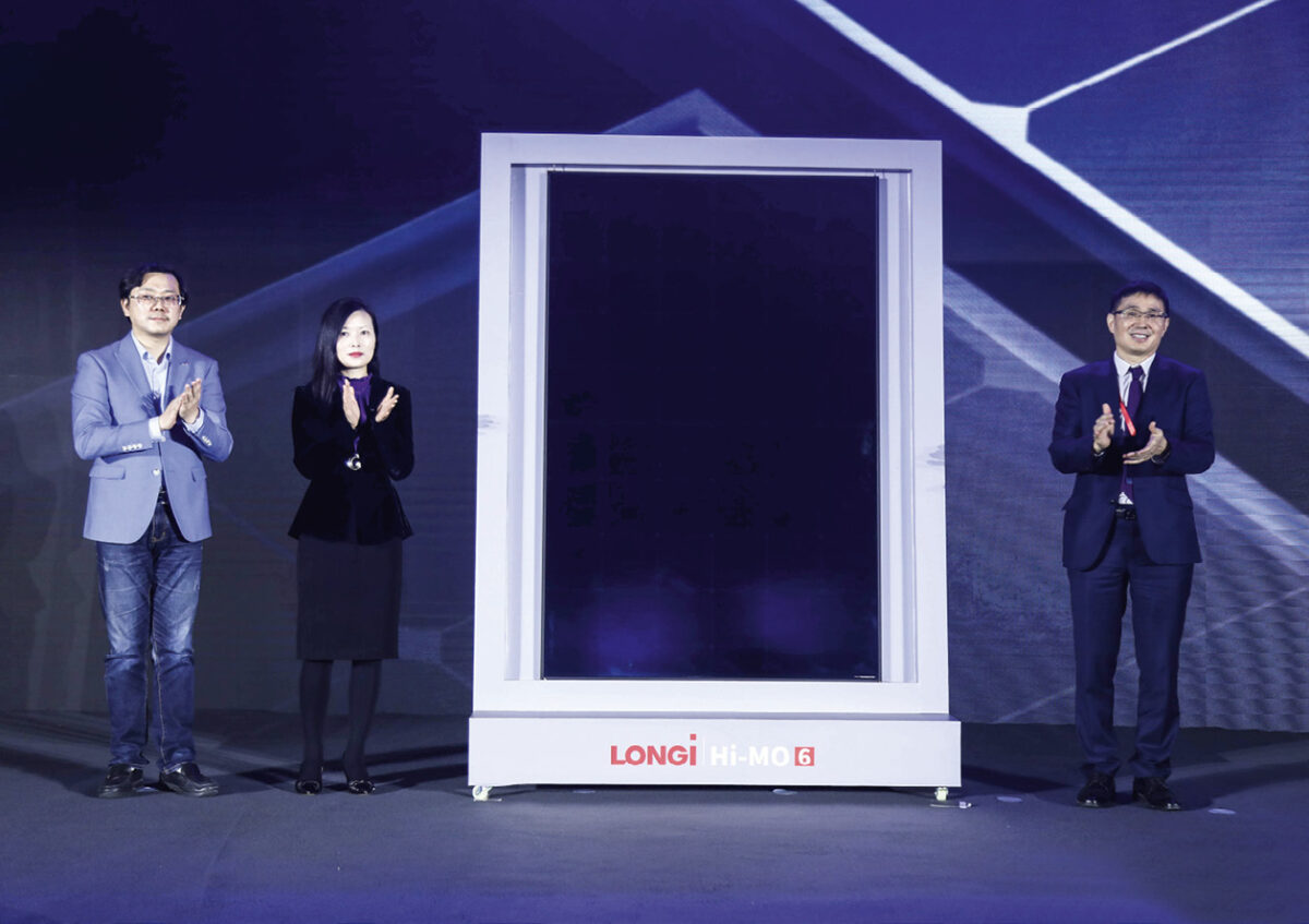
Chinese solar module manufacturer Longi plans to implement its back-contact solar cell technology in most of its panel production, as announced by the company’s chairman, Zhong Baoshen, during an investor meeting last week.
“Longi has a very clear view that in the next five to six years, back-contact cells will be the mainstream of crystalline silicon cells,” he said. “The high conversion efficiency of BC cells is the crown jewel of crystalline silicon technology, and the whole industry is ready now to pick this jewel.”
Longi plans to achieve a total solar cell production capacity of 110 GW by the end of 2023, with 30 GW dedicated to TOPCon technology and 80 GW for BC technology.
Baoshen stated a preference for BC cells over TOPCon devices, on claims that TOPCon cell technology is transitional and offers minimal efficiency improvements compared to past PERC technology advancements.
Additionally, BC technology can be combined with p-type wafers, for which Longi has substantial production capacities, giving it an advantage over the more common interdigitated back-contact (IBC) technology.
“The back-contact (BC) cell technology improves photoelectric conversion efficiency by shifting all the electrode grids on the front side to the back side of the cell, thus reducing the shading of the grids from sunlight.” Shen Wenzhong, secretary general of the Shanghai Solar Energy Association and Director of the Solar Energy Research Institute at Shanghai Jiaotong University, told pv magazine. “As a cell structure, BC technology can be combined with a variety of cell technologies to form back-contact based solar cells.”
In March, Longi launched its own hybrid passivated back contact (HPBC) tech. The company has yet to explain exactly what HPBC is, but it is believed to be an extension of p-type (positively doped silicon) IBC technology that combines the structural advantages of PERC, TOPCon, and IBC solar.
Longi will develop “P-IBC” cells using its extensive production capacity of p-type wafers, along with a silicon dioxide tunneling layer, polysilicon film, and upgraded laser equipment, low-pressure chemical vapor deposition, and coating-cleaning equipment—all derived from PERC-process lines.
This content is protected by copyright and may not be reused. If you want to cooperate with us and would like to reuse some of our content, please contact: editors@pv-magazine.com.





By submitting this form you agree to pv magazine using your data for the purposes of publishing your comment.
Your personal data will only be disclosed or otherwise transmitted to third parties for the purposes of spam filtering or if this is necessary for technical maintenance of the website. Any other transfer to third parties will not take place unless this is justified on the basis of applicable data protection regulations or if pv magazine is legally obliged to do so.
You may revoke this consent at any time with effect for the future, in which case your personal data will be deleted immediately. Otherwise, your data will be deleted if pv magazine has processed your request or the purpose of data storage is fulfilled.
Further information on data privacy can be found in our Data Protection Policy.