Although crystalline silicon solar cells possess many merits, including their material abundance, high power conversion efficiency and operating stability, as well as their mature production process, it has always been taken for granted that they cannot be used in flexible applications, because of the brittle characteristics of crystalline silicon wafers (Fig. 1). For this reason, silicon electronic devices are usually encapsulated by rigid glass and/or back sheets to form traditional monofacial or bifacial photovoltaic modules. These modules account for more than 95% of today’s photovoltaic market.
The path to foldable silicon wafers
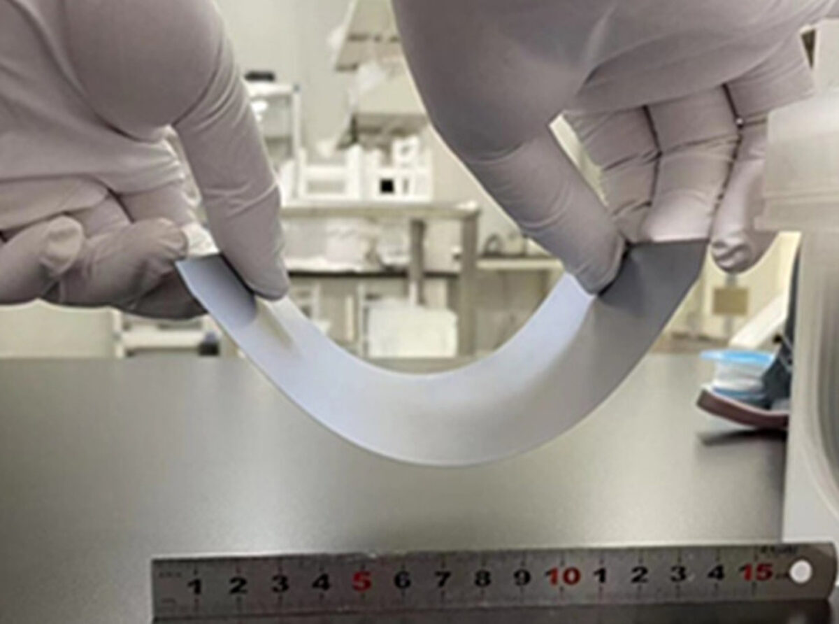
However, their low power-to-mass ratio impedes their installation on satellites, buildings, automobiles, clothes, and on other curved surfaces. My research team developed a strategy to fabricate foldable silicon wafers with a small bending radius of about 4 mm. When made into lightweight flexible amorphous-crystalline silicon heterojunction solar cells, the power conversion efficiency is independently calibrated to be more than 24% (Fig. 2). When the cells are encapsulated into a large flexible solar module (>10000 cm2), the power conversion efficiency reached 22,8%, much higher than other flexible counterparts made from cost-effective materials.
In comparison to standard bifacial modules encapsulated by glass, the weight-to-power ratio of flexible bifacial modules in this research decreases by about 95%, potentially paving the way for a large self-powered electronic market in the near future.
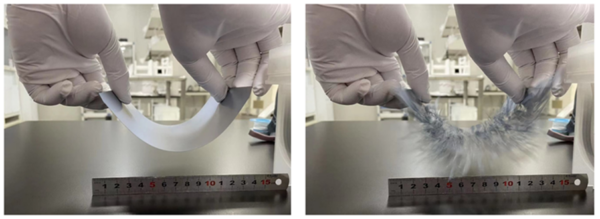
Image: IEC
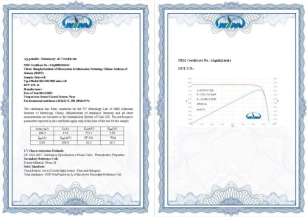
Image: IEC
Long term stability is an issue
For flexible applications, close attention should be focused on their long-term stability. For example, microcracks are induced during module encapsulation. More detailed examination reveals that these microcracks are located at the endpoints of solder strips (situated on the device edges). This suggests that maximum compress stress is applied when the endpoint of solder strips and the device surface come into contact. This is confirmed by a finite element analysis using the COMSOL Multiphysics software. Our research team proposed to blunt the pyramids on the wafer’s edges, and to convert the sharp V-shape channels to rounded U-shape channels between the surface pyramids. By dispersing the stress, this strategy reduced the maximum stress by about one order, enabling the solar cells to become more resistant to wafer deformation and frequent vibrations. The bending radius of an M2-size cell (156×156 mm) is less than 8 mm. When encapsulated into large modules of more than 2 m2, they can be rolled in a similar way to thin-film modules made from a-Si, organics, CIGS, CdTe and perovskite (Fig. 3). The least critical bending radius is less than 5 cm, indicating they are suitable for many niche applications. Moreover, these flexible solar cells are free-standing devices, unlike other thin-film cells deposited on expensive organic substrates or stainless steel.
The research group has demonstrated applications for high-altitude vehicles between a height of 10-100 km. In this range, the space radiation from ultraviolet rays and high-energy particles is not very challenging. More experiments should be conducted to estimate the impact of more extreme tasks before future deployment.
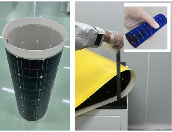
Image: IEC
Standards and testing are required
In this study, the research team also notes that there are no detailed test standards for flexible silicon photovoltaic modules. IEC Technical Committee 82, which prepares standards for solar PV energy systems, could lead work in this field. An experimental configuration for vibration tests is yet to be determined. The parameters for bending tests include bending radius and retention duration, and other test methods could include electroluminescence, photoluminescence, current-voltage analysis and so on. Finally, strain effect tests are recommended, because the tensile force applied may result in encapsulant failures, and destroy the conformal contacts between the encapsulant and the cell surface, as well as the conformal contacts between the solder strips and the cell surface.
Zhengxin Liu is an expert on solar cell materials and devices and measurement technology for solar cells. His current research interests include high-efficiency crystalline silicon solar cells, physics of heterojunction structures, as well as standardization of solar cells. He presents a summary of his research team’s breakthrough paper on flexible crystalline silicon solar cells, which was initially published in the journal nature.
The International Electrotechnical Commission (IEC) is a global, not-for-profit membership organization that brings together 174 countries and coordinates the work of 30.000 experts globally. IEC International Standards and conformity assessment underpin international trade in electrical and electronic goods. They facilitate electricity access and verify the safety, performance and interoperability of electric and electronic devices and systems, including for example, consumer devices such as mobile phones or refrigerators, office and medical equipment, information technology, electricity generation, and much more.
The views and opinions expressed in this article are the author’s own, and do not necessarily reflect those held by pv magazine.
This content is protected by copyright and may not be reused. If you want to cooperate with us and would like to reuse some of our content, please contact: editors@pv-magazine.com.



By submitting this form you agree to pv magazine using your data for the purposes of publishing your comment.
Your personal data will only be disclosed or otherwise transmitted to third parties for the purposes of spam filtering or if this is necessary for technical maintenance of the website. Any other transfer to third parties will not take place unless this is justified on the basis of applicable data protection regulations or if pv magazine is legally obliged to do so.
You may revoke this consent at any time with effect for the future, in which case your personal data will be deleted immediately. Otherwise, your data will be deleted if pv magazine has processed your request or the purpose of data storage is fulfilled.
Further information on data privacy can be found in our Data Protection Policy.