From pv magazine Global
A research group coordinated by the Netherlands Organisation for Applied Scientific Research (TNO) has investigated how cleaned wafers or wafer fragments recovered from end-of-life (EoL) PV modules could be reused for new crystalline silicon ingot production and has found that gallium-doped wafers could be particularly suitable for this purpose.
The scientists explained that silicon from the discarded wafers should be done by eliminating any contamination on its surfaces, which would re-include it in the high-purity material category. “The main contaminants are dopant, oxygen, carbon, and perhaps some nitrogen,” the research’s lead author, Bart Geerligs, told pv magazine. “We looked at this mainly from the perspective of dopant and resistivity control, and to a limited extent also from the perspective of other remaining contaminants.”
In the study “Potential for Recycled Silicon Solar Cells as Feedstock for New Ingot Growth,” published in Progress in Photovoltaics, the researchers explained that their analysis addressed potential technical and economic constraints related, in particular, to dopants and impurities. They also expect that significant silicon volumes may be recovered, especially from p-type wafers, from around 2040, and that boron-doped and gallium-doped markets will be more or less equally divided.
The research group also created a methodology to separate n-type and p-type modules, and boron-doped versus boron-doped or gallium-doped p-type panels. It established, for example, that if the solar cells in the module are polycrystalline, they are necessarily p-type B-doped. “To the best of our knowledge, there has been no commercial production of n-type modules based on polycrystalline silicon,” the academics said.
Furthermore, they created a separation between wafers that have front-side metallization or not. They also said that voltage should be identified for all modules except those based on interdigitated back-contact (IBC) cell technology, and that a visual inspection should be conducted on the rear side of all cells. “The principle for the inspection is then that all industrial p-type Al-BSF and PERC cells have Al-rear side metallization combined with local silver pads for soldering of the inter-connecting ribbons, and industrial n-type cells do not have such combination,” they specified.
The team explained that the whole testing scheme could be bypassed if a label on the discarded panel has useful information. “For example, a module could be documented as containing HJT cells (n-type) or be based on IBC cells from a manufacturer like Sunpower or Maxeon,” it further explained. “It would also be very helpful if PERC modules visibly show a production date because from before 2019, this would imply boron-doping, and after 2022, it would imply gallium-doping of the wafers.”
“This scheme would result in three material flows,” Geerligs said. “These are n-type doped cells, p-type boron-doped cells, and a flow of monocrystalline PERC cells that could be either boron-doped or gallium-doped.”
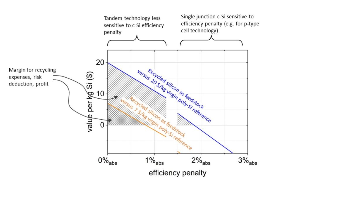
The scientists concluded that re-using p-type wafers as feedstock for new p-type ingots will not be economically viable, as n-type cells are now the dominant technology.
“The potential cost reduction from using recycled feedstock does not appear to be sufficient to compensate for this,” they stated. “Another possibility for a much better profitability for recycling of p-type wafers may become available with perovskite–silicon tandem technology, in which case both the efficiency disadvantage compared with n-type is strongly reduced and PERC cell performance can be enhanced by a poly- Si emitter.”
This content is protected by copyright and may not be reused. If you want to cooperate with us and would like to reuse some of our content, please contact: editors@pv-magazine.com.


This study highlights the promising potential of recycling gallium-doped silicon wafers from end-of-life solar panels for new ingot production.
By addressing contaminants and dopants, the research offers valuable insights into improving the economic viability of solar cell recycling.
However, the dominance of n-type technology suggests that the real cost-benefit potential lies in perovskite–silicon tandem technology for p-type wafer recycling.